Here you will find out latest app notes.
The Cadence® OrCAD® product suite offers a tightly integrated electronic design automation (EDA) environment. This environment supports complete system design flow starting from schematic capture to circuit simulation, and finally, PCB realization. Designers can reduce time to market, by leveraging seamless integration of OrCAD® Capture, PSpice A/D®, and OrCAD® PCB Editor. This application note also explains how designers can leverage simulation results to drive PCB layout.A robust and reliable power converter is essential for the success of any system design. This application note demonstrates the capabilities of PSpice A/D and how it integrates with other tools used in the complete design flow by taking a real life example and explains how designers can leverage simulation results to drive PCB layout.
A robust and reliable power convertor is essential for the success of any system design. The purpose of this design example is to demonstrate PSpice capabilities — its integration with other tools used in the complete design flow by taking a real life example.
ACDC VRM reference design covers the following aspects of design:
OrCAD Release 17.2 - 2016
The design goal is to develop a VRM module to meet the following specifications:
Input Voltage 110V (50Hz) , ±10%;
Efficiency at Full Load > 80%
Output Voltage: +48V, ±5%;
Maximum Output Current: 6Amp
Output Current Range: 1-6Amp
1A to 6A load Ripple voltage: 250mV P-P Max
Switching Frequency: ~150 kHz
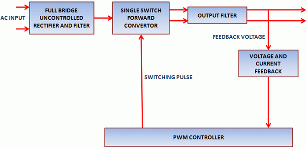
Single switch forward converter topology has been selected for this design. The high-level block diagram of this design is as follows:
Figure 1: VRM Block Diagram
Full bridge rectifier is used for rectification of the AC input to a DC output. This rectification is uncontrolled and may contain significant ripple. The ripple input voltage is a function of filter capacitor and load resistance.
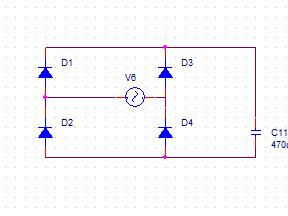
Figure 2: Full Bridge Rectifier
Figure 3 shows the conventional forward converter circuit. You will first understand how this circuit operates. When switch M1 is turned ON, current through the transformer winding starts building up. This current is equal to the transformer magnetizing current and the load current. At this time, diode D1 conducts and D2 is reverse biased. In this stage of switching cycle, energy is transferred to the inductor L3 and the load. When switch M1 is turned off, negative voltage appears across the transformer winding. This negative voltage makes D1 reverse biased and D2 forward biased. The energy stored in L3 and C1 continues to supply the load while current continues to flow through D2. This circuit does not show the RESET winding for primary magnetizing current. There are multiple methods for the same but these are not included in this note.
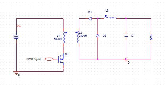
Figure 3: Single Switch Forward Converter
The output voltage in this case depends upon the Duty Cycle and the transformer ratio. Output voltage can be calculated using the following equation:
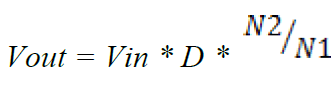
Where
N1 and N2 are the number of turns of transformer windings
General purpose offline PWM controller UC3843 is used in this application. This device is from a family of control devices that provide the necessary features to implement off-line or dc-to-dc fixed frequency current mode control schemes with a minimal external parts count. Internally implemented circuits include under-voltage lockout, featuring start up current of less than 1mA, a precision reference trimmed for accuracy at the error amp input, logic to insure latched operation, a PWM comparator which also provides current limit control, and a totem pole output stage designed to source or sink high peak current. The output stage, suitable for driving N-Channel MOSFETs, is low in the off state.
Limitation
This is a conceptual design created to demonstrate capabilities of the tool.
First step of the design procedure is to verify block-level implementation and gather high-level specification for various devices required for real life implementation. For that you will capture the block diagram shown in Figure 4 using ideal devices. Ideal devices can be found in following three libraries:
Components from these libraries are meant for basic design simulation in ideal conditions. These components do not have any limitations, such as switching delays, leakage inductances, and winding resistances.
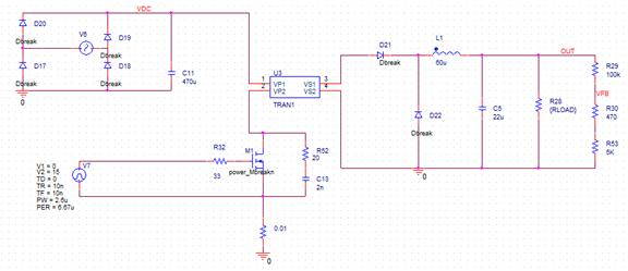
Figure4: VRM Circuit
Figure 5 shows the current waveform through various power devices.
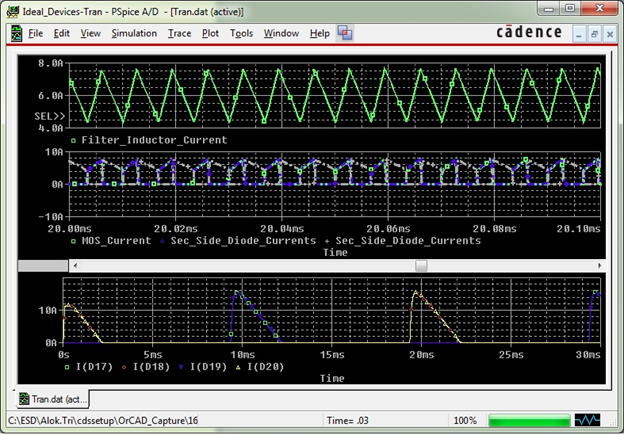
Figure 5: Current Through Various Power Devices
After identifying the various device ratings, you will replace the ideal devices with actual models, and perform simulation and measurement for various design parameters. In this simulation, transformer realization has been done using linear coupling parameters. The simulation, therefore, does not exhibit any magnetic saturation characteristics. Since this is an ideal coupling, RESET circuit of forward convertor has also not been included. However, in PCB layout stage RCD type of RESET windings have been used for completeness.
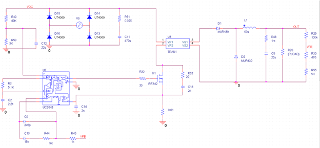
Figure 6: VRM Circuit with real devices
You can adjust the output filter capacitor to meet the desired voltage ripple. Figure 7 shows the output voltage ripple.
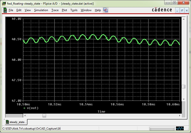
Figure 7: Output Voltage Ripple
Figure 8 shows the current through various power devices. Observe the current through various devices. The result can also be used to co-relate this simulation result with simulation result for ideal devices (Figure 4) to see the effect of actual devices models and change in various output. This analysis is useful to select devices with appropriate parameters, for example if MOSFET peak current has gone up significantly, you might see the reverse recovery time of diode used in secondary side and might decide to go for a device with lower stored charge or faster recovery time.
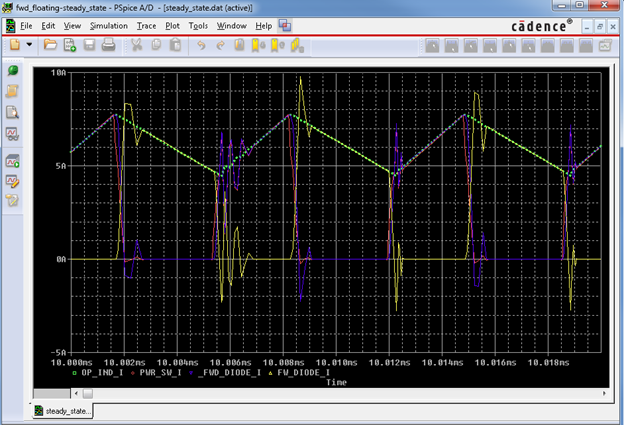
Figure 8: Line regulation - Current through various power devices
You can also simulate the design at light load condition to check if continuous conduction mode (CCM) is maintained for complete range of operation. You should select the maximum input voltage and minimum load current to observe the worst case situation in this context.
Now let’s simulate the design to find out the line regulation of this voltage regulation module. To get the line regulation of this VRM we need to simulate the design with known input voltage variation and measure the output voltage against this input variation.
In this setup (refer figure 9) you will notice that an additional voltage source V7 has been added to the input. The purpose of this voltage source is to simulate the effect of input voltage fluctuation. This is also used for measurement of VRM performance under fluctuating line conditions. To perform this measurement under various load conditions, simulation setup includes parametric sweep for load
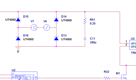
Figure 9: Input Line variation
resistance. In order to perform parametric sweep analysis make the following two changes in the design.
1. Set the component value as variable (refer figure 10): Edit the component value onto schematic and set it’s value as {PARAMETER NAME}; for example {RLOAD}
2. Define PARAMETER NAME as variable in schematics: Place the PARAM component (available in special.olb) onto schematic. Select and edit properties. Add New Property. Define Property name as RLOAD and set a default value. Then configure the simulation profile to sweep this parameter.
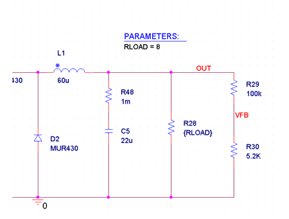
Figure 10: Configuring design for parametric sweep
In order to perform parametric sweep, we need to configure simulation profile to run this analysis. In this case simulation profile (figure 11) has been configured to simulate load current of 6Amp, 3Amp, and 1Amp (8Ω, 16Ω, 48Ω).
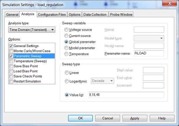
Figure 11: Parametric Sweep-Simulation of Various Load Conditions
Simulation results after configuring design and running the analysis are shown in figure 12. These waveforms show the following:
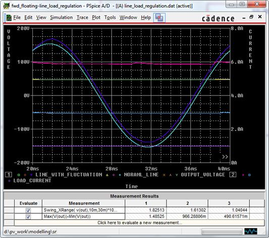
Figure 12: Static Line & Load Regulation
You can also configure measurement expressions to quickly and easily perform these measurements. To measure maximum variation in output voltage, you can use the Swing_XRange measurement expression. For this example, the expression should be Swing_XRange (V(out),20m,40m). You can also directly calculate the regulation in percentage (%) by using Swing_XRange(v(out),20m,40m)*100/YatLastX(avg(v(out))). Using this expression the calculated value for load or line regulation comes out to be < 2%.
Estimation of accurate switch loss is a very crucial aspect of a successful VRM design. This directly influences the reliability of power supply under various operating conditions, and also drives the heat sinks selection and thermal design.
In hard switching topologies the switching losses are crucial factor and cannot be ignored. There is no direct method to obtain these accurately from datasheets and losses are very sensitive to circuit parameters and parasitic. You need to first understand the switching loss in MOSFET. Switching loss in MOSFETs is due to simultaneous application of high voltage and high current through the device. As shown in picture below, the MOSFET drain current has been building up while voltage across drain to source is yet to drop, leading to a finite loss across the switch. Amount of switch loss can be estimated by area enclosed by voltage and current (RED & BLUE) waveforms as shown in following diagram.
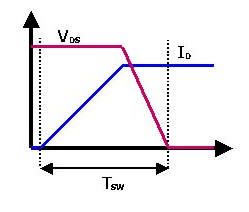
Figure 13: Switch Loss in Hard Switching Condition
Another type of loss in MOSFET is conduction loss or loss in switch when it is conducting. As high voltage MOSFETs devices have high RDS, this loss can also be significant. This is also known as the Ohmic loss.
You can use simulation to accurately estimate losses in power devices and tune gate resistance and other circuit parameters to optimize the design.
In figure 14, the topmost waveform plot is average switch power loss; the middle waveform is instantaneous switch power loss, and the bottom waveform is switch current and voltage waveforms. Average switch power loss is integration of instantaneous power loss over time. This can be performed using integration S function in PSpice.
Similar approach can be adopted for estimation of power loss in other devices.
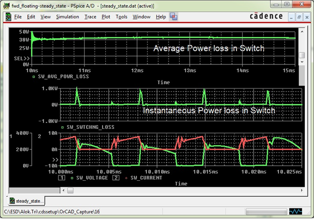
Figure 14: Switch Power Loss
You can directly calculate the average power drawn from a source using the average function and delivered to load. Using these two measurement, efficiency of VRM can be calculated. In order to obtain reasonable accuracy, you should perform such measurement on simulation done in steady state covering at least three to four cycles. Figure 15 display the input power and power delivered by VRM (output power)
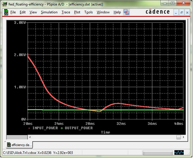
Figure 15: Efficiency Calculation
VRMs may need to supply current to loads that are transient in nature. Such sudden loading or unloading of VRM may pose an additional challenge for the VRM controller. Sudden transients can even trip the VRM or its output may swing outside the specified range. Such situation necessitates the simulation of VRM under transient load conditions. This is done by simulating step load change at the output of VRM and variation in output voltage, and performance of feedback loop can be verified under various operating conditions. In order to simulate step load response additional circuitry has been added to simulate transient load. This additional circuit (refer figure 16) creates 33% step jump in load current and after some time (5mSec) this additional load is disconnected. Load Step_Current_Responce display setting to see the load current variation and its impact on output voltage.
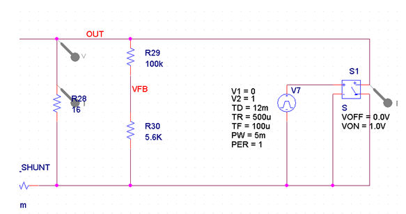
Figure 16: Additional circuit to simulate step load responce
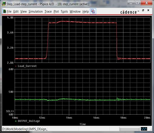
Figure 17: Step Response
These responses would also depend upon feedback loop response and bandwidth. You can use these measurements to fine-tune feedback loop or compensator parameters to get desired response from the system.
Any conventional SMPS has capacitive filter connected at input rectifier stage. Due to this, current drawn from mains is very irregular in shape, contain high amplitude, and are of short duration. This nature of current waveform creates severe stress on the input mains system and can lead to potential system issues or non-compliance to regulatory standards. Two parameters Power factor (PF), and Total Harmonic Distortion (THD) are used as qualitative measure for this purposes. Both of these measurements can be performed using PSpice.
One can perform Fourier analysis using PSpice to get harmonic distortion of VRM input current. This can be done by selecting the Fourier analysis option under simulation setting (refer figure 18). You can define voltage node or current through a device, for which this analysis need to be performed. The results of this analysis can be viewed in the simulation output file. The Fourier analysis result for this VRM at full load condition is given below.
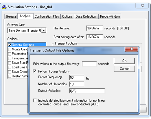
Figure 18: Fourier Analysis result at Full load
FOURIER COMPONENTS OF TRANSIENT RESPONSE I(V_V6)
DC COMPONENT = 1.588979E-02
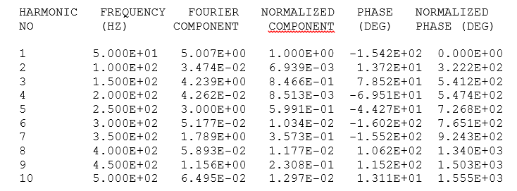
TOTAL HARMONIC DISTORTION = 1.121256E+02 PERCENT
If you observe these results carefully, you will find that contributions of the even harmonics (2nd, 4th, and so on.) are significantly less compared to the odd harmonics (3rd, 5th, and so on.). This is as expected because current waveform exhibits half wave symmetry.
You can also view the Fourier spectrum of any waveform loaded in probe.
Similar approach can be used to perform the simulation for various other important VRM specifications, such as:
o Against the EN61000-4-11 standards
Against the EN61000-3-2, EN61000-3-3 standard
The design of a switching power converter is only as good as its layout. This necessitates very close co-ordination between the circuit designer (simulation expert) and the layout designer throughout the design and prototype phase. Once various design parameters of VRM have been verified, design can be taken to the layout stage. One of the key challenges in Switch mode power supply design implemented on boards is having proper trace width and trace clearances for various connection handling high voltage and high current. Simulation results can be leveraged to decide proper trace width and clearances as per actual current and voltage through them. This can save prototype testing phase, can help cut down both time to market, and the cost incurred in prototypes. In this design, trace width and trace clearance have been assigned based on simulation results.
Trace width calculation for output can be done as following. These calculations are based on IPC-2221/IPC-2221A design standards.
Copper thickness = 1oz/ft2
Temperature Rise = 20°C
Max Current = 6Amp
Required Trace Width = 2.34mm (External trace)
Max Current = 4Amp
Required Trace Width = 1.33mm (External trace)
After the calculation of various trace clearance parameters the MIN_LINE_WIDTH property should be set on the respective nets.
Trace clearance calculation for nets involving high voltages can be done as following. These calculations are based on IPC-2221/IPC-2221A design standards.
Max Voltage = ~250V
Required Trace Clearance = 1.25mm (External trace; uncoated)
Required Trace Clearance = 0.4mm (External trace; coated)
After the calculation of various trace clearance parameters, you should set SPACING Constraints on respective nets.
In addition to the above two parameters, you can also leverage the simulation results to drive the placement of devices which are dissipating power and keeping temperature sensitive parameters in different zone. Similarly, simulation result can be used to identify the nets with high di/dt or dv/dt and special precaution can be taken while routing these nets.
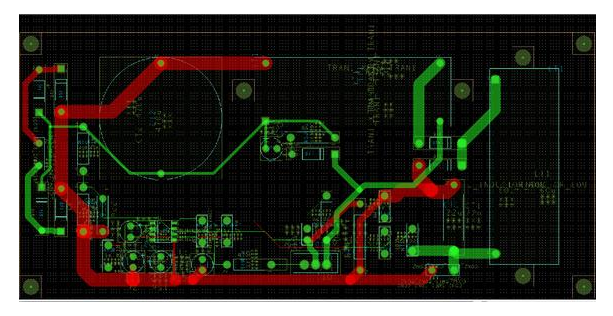
Figure 19: PCB Layout Figure
This application note highlights some of the benefits of using Cadence® OrCAD® suite and the capabilities of PSpice for designing and optimization of various designs parameters for a Voltage Regulator Module. PSpice A/D®, the simulation and analysis tool of OrCAD® products, comes with a comprehensive built-in device library and simulation models for complex devices such as PWMs. Using these models, designers can simulate complete closed loop systems and fine-tune transient response of a system. Tight integration of OrCAD tools facilitate design flow tasks and offer several advantages to designers. Some of these advantages are:
These advantages are amplified when teams or vendors distributed across the globe adopt the same tools and the same approach.
© Copyright 2016 Cadence Design Systems, Inc. All rights reserved. Cadence, the Cadence logo, and Spectre are registered trademarks of Cadence Design Systems, Inc. All others are properties of their respective holders.
1766 12/13 CY/DM/PDF
Copyright © 2020 Cadence Design Systems, Inc. All rights reserved.